A Low Noise Audio TIA
Motivation
This is the 1st revision of the TIA circuit that was used with the field mill sensor described here.
Device Selection
A 2SC2714-O NPN transistor was selected as the gain element of the transimpedance stage, mainly for its 2.5 dB noise figure (measured at 100 MHz, Ie = 1 mA).
Part Statistics
| Number | Max Vce (V) | Ft (MHz) | Max Ic (mA) | Min hFE | Max hFE |
|---|---|---|---|---|---|
| 2SC2714-O | 30 | 550 | 20 | 70 | 140 |
SPICE Model
.MODEL 2SC2714 NPN( IS=1.45E-15 BF=166 NF=1.00 VAF=71 IKF=49E-3 ISE=43E-15 NE=2.45
BR=5.33 NR=997E-3 VAR=22 IKR=69E-3 ISC=847E-18 NC=1.02 RB=14 IRB=1.00E-6 RBM=14
RE=46E-3 RC=9.17 XTB=0.00 EG=1.11 eV XTI=3.00 CJE=1.66E-12 VJE=717E-3 MJE=331E-3
TF=153E-12 XTF=100 VTF=383E-3 ITF=90E-3 PTF=47 CJC=781E-15 VJC=630E-3 MJC=462E-3
XCJC=1.00 TR=1.00E-6 FC=900E-3)
Bias Point
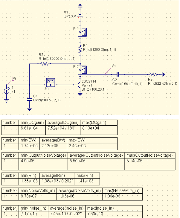
Assume a Vcc of 3.3 V, for compatibility with 1.5 V and 3.6 V battery cells. Choose Vce = 2 V, Ic = 1 mA for an approximate 2 Vpp output swing and a low noise figure (the BJT only seems to be specified for Ic = 1 mA in the datasheet). The collector-feedback bias circuit needed to achieve this (as calculated in AppCad) is: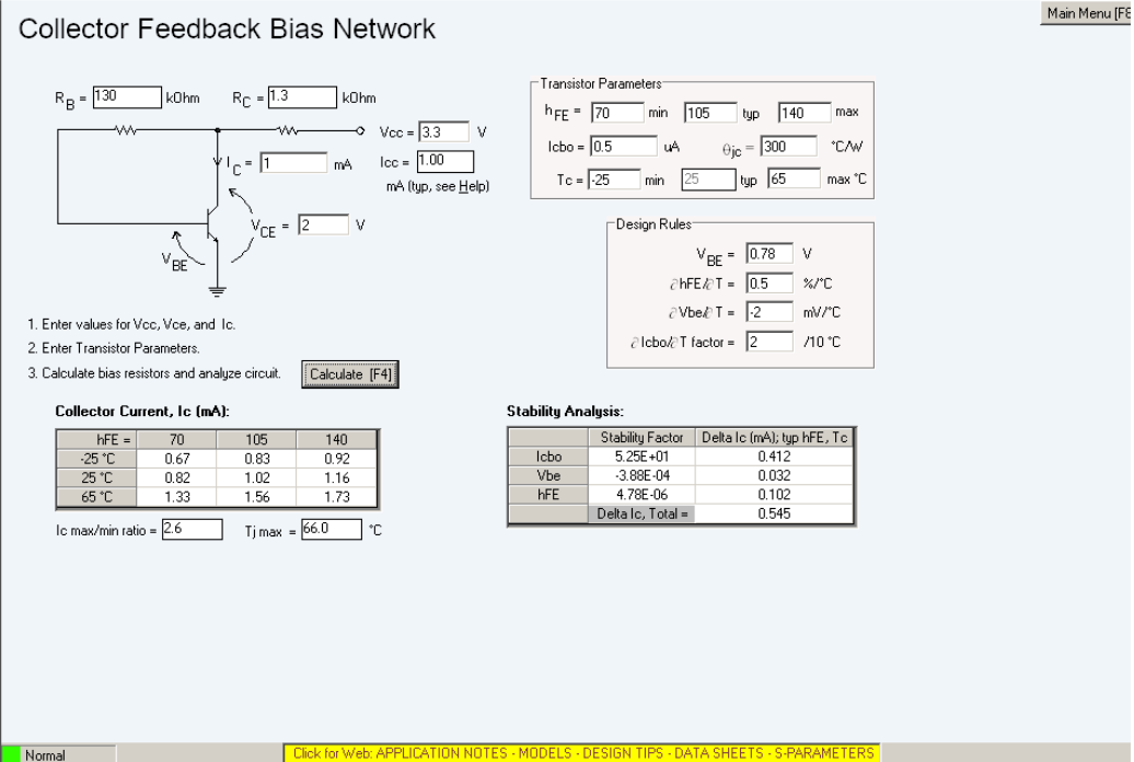
Circuit Topology Small Signal Analysis
BJT Hybrid Pi Model
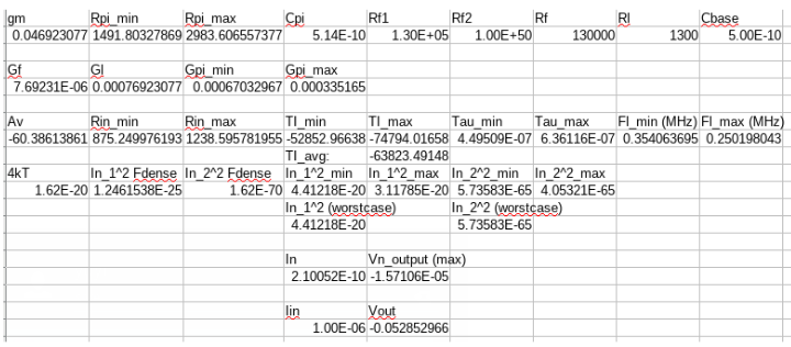
| Ic (mA) | Ft (MHz) | gm (mOhms^-1) | Cpi (pF) | Min hFE | Max hFE | Min Rpi (Ohms) | Max Rpi (Ohms) |
|---|---|---|---|---|---|---|---|
| 1 | 550 | 38.4 | 11 | 70 | 140 | 1822 | 3645 |
Circuit Topology
Assume a shunt-feedback topology for convenience: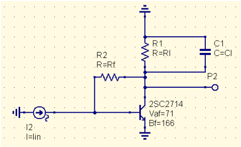
The DC gain is: \[\frac{V_o}{V_i}=\frac{G_f-g_m}{G_f+G_l}\] The input resistance is: \[R_{in}=\frac{R_{\pi}}{1+R_{\pi}G_f(1-A_v)}\] The DC transimpedance gain is: \[\frac{V_o}{I_i}=\frac{A_vR_{\pi}}{1+R_{\pi}G_f(1-A_v)}\] For a large \(A_v\), this gain formula reduces to \(R_f\). From the perspective of \(C_\pi\), the circuit time constant is: \[\tau_1=\frac{C_\pi}{g_m+g_\pi+G_lA_v}\] From the perspective of \(C_l\), the time constant is: \[\tau_2=\frac{C_l}{G_l+(1+\beta)(\frac{1}{R_f+R_\pi})}\] The dominant pole then has a time constant of \(\tau=\tau_1+\tau_2\). The input noise current can be calculated from \(R_f\): \[i_n^2=4kT\times F_{3dB}/R_f\] where \(4kT=1.62\times10^{-20}\) at 20 deg C. To account for additional resistors in parallel with \(R_f\), note that the noise current powers simply add.
Audio Amplifier Stage Design
To convert the TIA output into an audio line level signal, use an appropriate audio amp IC:
| Part Num | Input Voltage Range | Load Impedance | 1% THD Pout with Vdd=3.3 V |
|---|---|---|---|
| LM4818 | -0.3 V to VDD+0.3 V | 16 Ohms | 120 mW |
We want a large input resistance with respect to the BJT collector resistance and a moderate gain so that the LNA’s noise figure is dominant. For this, choose \(R_{in}=22\ k\Omega\) and a gain of 3 V/V. It is desirable for the passband to omit 60 Hz (powerline frequency). Therefore, choose a bandwidth of 70 Hz to 20 kHz.
The general circuit for the LM4818 is: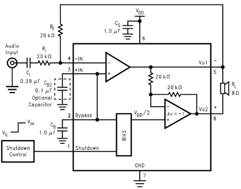
\(R_i\) is simply the desired input resistance (22 kOhms). Since \(A_v=2(R_f/R_i)\to 1.5=R_f/R_i\), \(R_f=33\ k\Omega\). Set the 3dB frequency of the \(R_i+C_i\) high-pass element to \(0.2\times 70\ \textrm{Hz}\). Therefore, \(C_i>0.517\ \textrm{uF}\). The resultant component values are:
| \(R_i\) | \(R_f\) | \(f_l\) | \(f_h\) | \(C_i\) | Required GBWP | \(C_B\) | \(C_{B2}\) | \(C_s\) |
|---|---|---|---|---|---|---|---|---|
| \(22\ k\Omega\) | \(33\ k\Omega\) | 14 Hz | 20 kHz | 0.56 uF | 300 kHz | 1 uF | 0.1 uF | 1 uF |
LNA Component Value Calculations
In QucsStudio: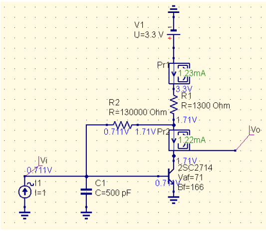
3.3 V Supply
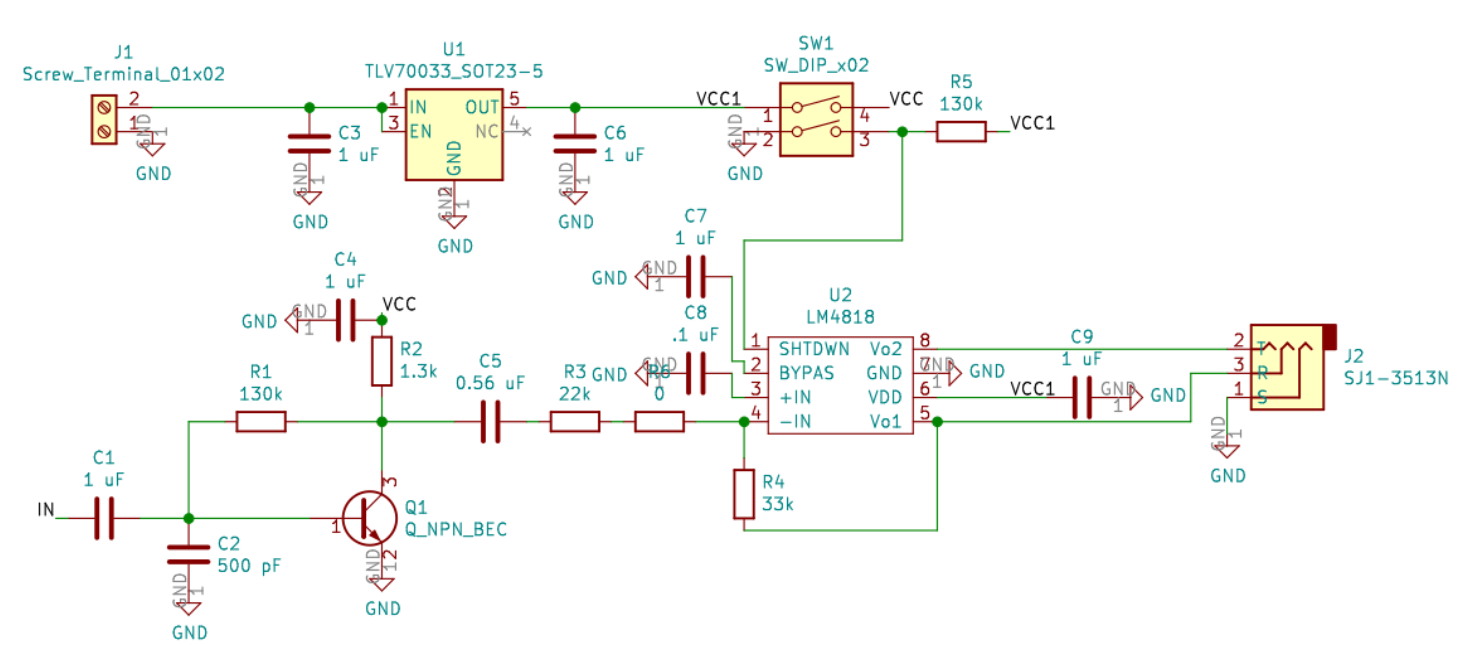
A 3.3 V LDO (TLV70033) was found on Digikey to supply the needed voltage.
Layout
Schematic
PCB
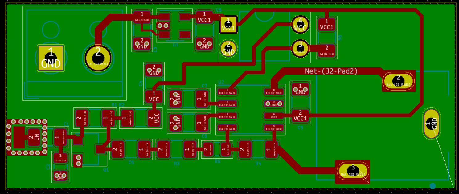
Note the usage of a grounded guard ring for shielding the input. The previous TIA design had a relatively high input resistance, increasing its sensitivity to E-field noise (which appears as a noise current in shunt with the input). Although this isn’t the case for the current revision of the circuit, it’s almost always better to shield high gain inputs.